
A copper inlay PCB with massive copper inserts for high current-carrying capacity and efficient heat dissipation in power and high-current applications.
Copper Inlays | PCB | High Current Circuit Boards
Copper Inlays
Copper inlay PCBs are a special circuit board solution in which massive copper inserts (inlays) are directly integrated into the board. This technology is primarily used to safely conduct high currents and effectively dissipate heat, which is crucial in power and high-current applications. Typical areas of use include power converters, automotive electronics, power modules, or industrial drives.
In short: copper inlay PCBs are the solution when standard conductor tracks are no longer sufficient for current or thermal management.
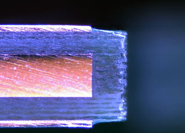
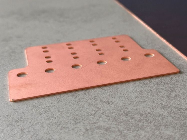
The manufacturing process of copper inlay PCBs is similar to that of standard multilayer boards. However, before lamination, the inlay areas (“pockets”) must be milled out in the inner layers. Copper pieces of the corresponding shape are then manually inserted into these pockets.
Several prepregs with a higher resin content ensure during lamination that the copper inlays are precisely fixed and that the gaps to the inner layer are completely filled with resin.
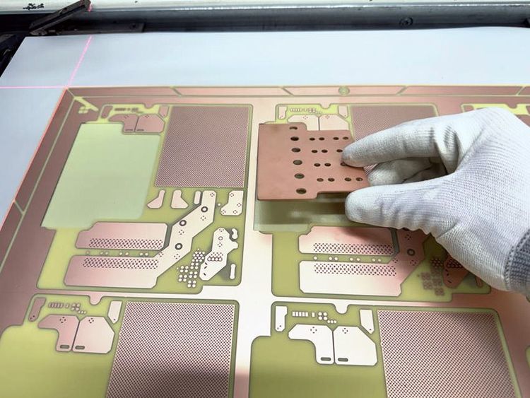
After lamination, the PCB is processed further using conventional methods. Plated-through holes into the copper inlays are, of course, possible.
Advantages of Copper Inlay PCBs
- Excellent current-carrying capacity
- Improved heat dissipation
- High mechanical stability
- Longer service life of the assembly
Disadvantages of Copper Inlay PCBs
- High manual manufacturing effort
- Expensive (material & production)
- Heavy, depending on the amount of copper
- Design limitations (layer, size, precision, etc.)