
With simple depth-milling a standard printed circuit board can be prepared for flexible installations. So called "semi-flexible" printed circuits are offering a cost-efficient solution.
Semi-Flex PCB | Flex-to-Install | Depth-Milling
Semi-Flex PCB Technology – Flexible Installation Without Connectors
Often layout designers are reluctant to upgrade from a standard PCB with connectors to a notoriously expensive rigid-flexible printed circuit. The advantages are immense, but so are the costs and the layout requirements compared to standard PCBs. Many times this "jump" from standard technology to a high-tech segment is not necessary. Many printed circuits do not require dynamic bending capabilities in operation but only need to be fit into the housing neatly. This is called a "flex-to-install" requirement and here semi-flex offers a really cost-saving alternative technology.
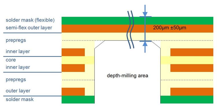
Production of a semi-flexible PCB is identical with the manufacturing process of standard printed circuits. Semi-flexilbe boards can be produced as single-layer, double-layer or multilayer PCBs. With the exemption of a special solder mask that sustains bending, the materials are also identical to standard printed circuits. The only difference happens at the end of the production process when dedicated bending areas are milled down by z-axis routing. The remaining material can be bend and is thin enough to only carry the copper traces and little base material.
To optimize transportation-safety and assembly, semi-flexible PCBs should always be produced in panels. You can easily seperate the prints from the panel after assembly and install the boards.
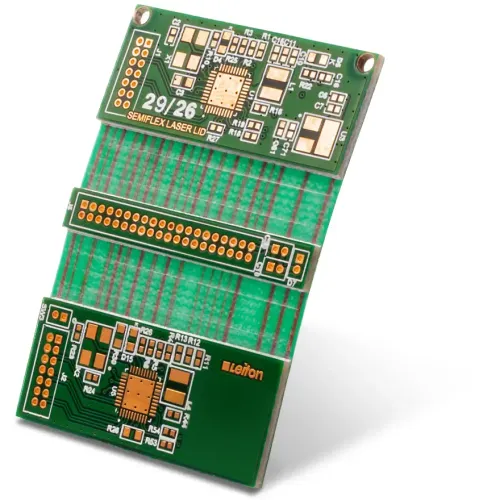
Design and installation of semi-flexible PCBs require some attention and modifications
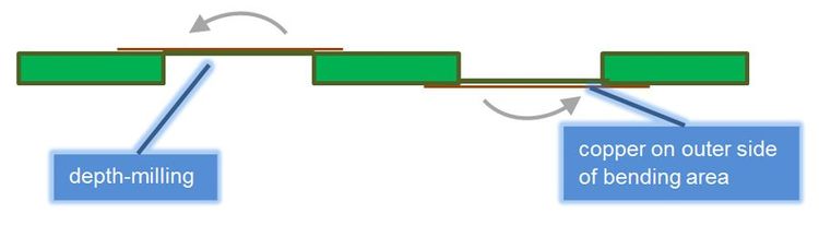
1. The PCB should only be bend with copper on the outside of the bending area.
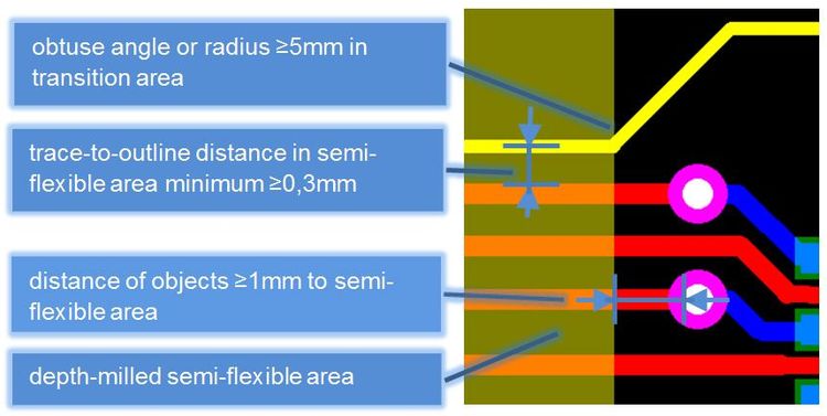
2. Open copper structures, pads, annular rings or vias in the rigid part of the PCB should have a distance of at least 1mm from the bending area. In special cases 0,8mm are okay, too. The semi-flexible are cannot contain any vias, drills or open copper structures. The transition area from flexible to rigid should have a radius of 5mm or an obstuse angle. Trace-to-outline distance in the semi-flexible area should be minimum 0,30mm.
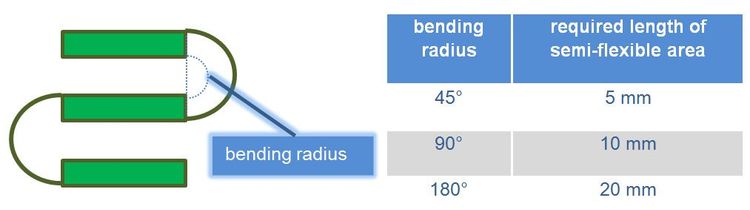
3. The maximum bending radius depends on the lenght of the semi-flexible area.
4. Currently, semi-flexible PCBs are possible up to 8 layers, while only one outer layer can be "semi-flexible" per bending area.
5. For the bending process we reommend to do this under hot air (you may use a hair dryer) and bend it over a fixed object in order to do so evenly.
| Characteristic | Values, description |
|---|---|
| material type | FR4, Tg 130°C and some high-Tg materials up to 170°C |
| remaining material | 150µm to 250µm |
| maximum beding radius | 180°, depending on semi-flex area |
| copper thickness | 35µm |
| maximum layers | rigid area up to 10 layers, semi-flexible area one layer (outer) |
| solder mask | flexible solder mask, green (for beding) |
| bending | flex-to-install, not suitable for dynamic bending |
| prints | partial silk print or other solder mask colours possible, not receommended in bending area |
| depth-milling | digital z-axis milling, camera controlled, tolerance +/-20µm |
When to use Semi-flex PCBs
Applications
Folded assemblies
compact housings where the board is installed bent over edges or levels.
LED and lighting technology
light strips and modules routed around housing edges and radii.
Power supplies and industrial electronics
replacement of board-to-board connectors and cable bridges between two rigid sections.
Automotive and displays
display, control and camera modules where the display plane is angled to the main board.
Sensor technology
sensor plane angled or offset from the evaluation electronics, without an additional connector.
Comparison
Semi-flex versus Flex and Rigid-flex
| Solution | Construction | Bending | When it is the right choice |
|---|---|---|---|
| Semi-flex | FR4, depth-milled to 150 µm to 250 µm remaining thickness, up to 10 layers in the rigid section, one outer layer in the bend area | One-time bend for installation, up to 180°, not dynamic | Installation with a single bend, cost advantage over rigid-flex and connector solutions |
| Flexible PCB (FPC) | Polyimide, 1 to 6 layers, material thickness 12.5 µm to 65 µm without copper | Static and dynamic, millions of bending cycles with a suitable design | Moving assemblies, cable replacement, tightest installation space |
| Rigid-flex | Rigid FR4 plus flexible polyimide in one compound, 2 to 12 layers | Static and dynamic | Several rigid sections in one compound, miniaturisation, three-dimensional installation, highest reliability |
Semi-flex is not designed for dynamic bending loads.
Material selection for semi-flex – why fillers and high Tg are harmful in the bend area
The bendability of a semi-flex PCB is created in the depth-milled remaining material of 150 µm to 250 µm. What matters there is the elongation at break of the resin, not the Tg value (glass transition temperature). High-Tg materials reach their Tg through more densely cross-linked resin systems. Densely cross-linked resins are harder and more brittle. Many high-Tg and halogen-free materials therefore also contain mineral fillers. Fillers reduce the elongation at break and significantly increase the risk of fracture in the bend area. For semi-flex, a high Tg value is therefore not a quality feature but a risk factor.
Typical reasons for fillers in a base material are at the same time warning signs for the bend area:
- Halogen-free flame retardancy: flame protection without bromine requires mineral fillers, for example aluminium hydroxide.
- Reduced CTE (coefficient of thermal expansion): fillers reduce z-axis expansion in favour of reliable plated through-holes.
- CAF resistance (conductive anodic filament): CAF-optimised material classes are frequently filled.
If one of these properties is highlighted in the datasheet, the material is usually filled and unsuitable for the bend area.
In the bend area, Leiton uses unfilled FR4 with Tg 130 °C as standard. This resin is more ductile. During installation, the bend area can also be brought close to its softening point by applying heat, which makes the bend process-reliable. With Tg 170 °C this effect is hardly achievable with simple heating. If the assembly requires high Tg for thermal reasons, Leiton reviews the build-up in advance: material type, filler content, remaining thickness and bend radius are then defined together.
Advantages
Cost advantage
standard FR4 process with depth milling, no polyimide compound as with rigid-flex.
Reliability
no plug contacts between the rigid sections, fewer failure sources under vibration and during assembly.
Simple installation
bend once, install, done (flex-to-install), no special tooling.
Functional density
up to 10 layers in the rigid section; the bend area only costs one outer layer.
One component instead of three
board, cable and connector combined into a single assembly.
Important notes
The bend area is designed for the one-time bend at installation only, not for dynamic loads. Exposed copper structures, pads, annular rings and barrels must be at least 1 mm away from the bend edge. The bend radius depends on remaining thickness and bend angle; at 200 µm it is around 4 mm.
| Design rules of thumb |
R = 20 × remaining thickness L = α / 180° × π × R + 2 × board thickness |
|---|
The bend must not start directly at the milled edge. The allowance of twice the board thickness acts as straight run-out behind the milled edges. Table values are approximate values for 1.6 mm board thickness, rounded up to full millimetres.
| Remaining thickness | Smallest possible bend radius | Bend area length at 45° | Bend area length at 90° | Bend area length at 180° |
|---|---|---|---|---|
| 150 µm | 3 mm | approx. 6 mm | approx. 8 mm | approx. 13 mm |
| 200 µm | 4 mm | approx. 7 mm | approx. 10 mm | approx. 16 mm |
| 250 µm | 5 mm | approx. 8 mm | approx. 12 mm | approx. 19 mm |
Printing in the bend area is not recommended. The bend area is finished with flexible solder mask (green). High-Tg materials and especially filled or halogen-free systems increase the risk of fracture in the bend area. They can only be used after a technical review of the build-up (see the material selection section). Cost drivers are layer count, depth-milled area and tolerance requirements (digitally controlled depth milling, tolerance +/-20 µm).
Compliance documents such as RoHS and REACH are available on request.
Request and Calculate semi-flex PCBs
What we need for a reliable quotation: layout data (ODB++, Extended Gerber, KiCAD or similar), position and width of the bend area, bend angle and required bend radius, layer stack-up, quantities and target dates. Leiton places each project appropriately based on price, lead time and technology.
Why Leiton: engineering support for the bend area design, manufacturability check before production, prototype to series, express production, call-off frame orders and direct personal contact.
Frequently Asked Questions
about Semi-flex PCBs
- When is semi-flex the better choice over rigid-flex?
When the board is bent only once for installation. Semi-flex uses standard FR4 with depth milling and is therefore considerably more economical than the rigid-flex compound of FR4 and polyimide. For dynamic bending there is no way around flex or rigid-flex.
Can a semi-flex PCB be bent more than once?The bend area is designed for the one-time bend at installation (flex-to-install). 5 to 10 bends are possible, which is always sufficient for installation and rework. If a design requires more bending, semi-flex is the wrong technology. Flex or rigid-flex is the right choice then.
Which bend radius and bend angle are possible?Bends up to 180° are possible. The smallest possible bend radius depends on the remaining thickness (150 µm to 250 µm) and follows the rule of thumb 20 × remaining thickness: 3 mm at 150 µm, 4 mm at 200 µm, 5 mm at 250 µm.
Which layer counts are possible?Up to 10 layers in the rigid section. One layer runs through the bend area on the outer side.
What drives the cost of a semi-flex PCB?Layer count, size of the depth-milled area, tolerance requirements and quantity. Compared to rigid-flex, the polyimide material is eliminated, which is the main cost advantage.
Which materials are used?FR4 with Tg (glass transition temperature) 130 °C as the unfilled standard in the bend area, selected high-Tg materials up to 170 °C after technical review, copper 35 µm, flexible green solder mask.
Why does Leiton use standard Tg 130 in the bend area instead of high Tg?Because the resin is more ductile. High-Tg systems are more densely cross-linked and often filled; both make the remaining material more brittle and prone to fracture. In addition, Tg 130 material is easier to bend with applied heat during installation. Details in the material selection section on this page.
Which other names are common for semi-flex?Semiflex, semi-flex PCB, semi-flexible PCB, flex-to-install PCB. All of these refer to the depth-milled FR4 solution, not to a polyimide flex circuit.