Printed circuits with double sided 400 µm copper are without doubt the king of high-copper-clad PCBs. Using such massive copper cladding you can use high currents on your PCB without challenging putting strain on your electronics.
400 µm Microvias | HDI | High Signal Density | Miniaturization | Sequential Build-Up (SBU) | Stackup Optimization
400 µm Microvia Technology – Ultra-Fine HDI PCBs for High Signal Density
Printed circuits with double sided 400µm copper are without doubt the king of high-copper-clad PCBs. Using such massive copper cladding you can use high currents on your PCB without challenging putting strain on your electronics. The challenge in printed circuit board production of such 400µm PCBs lies in a uniform etching and in applying an even and smooth solder mask that is covering the edges properly.
Extremely high currents on printed circuits require thicker copper cladding so that the induced heat-up of traces does not destroy the PCB. Although sometimes much thicker stack-ups are desired, we can implement two 400 µm copper layers into a standard PCB with 1,6 mm total thickness. So apart from a substantially heavier PCB the space requirements remain the same.
We use FR4 Tg 150°C material with a dielectric strength of around 3 kV per 100 µm. Other materials are possible in enquiry, as we keep 400 µm base copper on stock and can combine it with any material. Multiple etching runs are necessary to etch 400 µm PCBs. This leads to some layout restrictions. You can find the current limits on this technology in our rigid PCB technology section, as we continuously thrice to push the limits further.
One thing to consider during a 400 µm layout design is that the traces need to be much wider than usually. Commonly, traces need a base width that is factor 2 to 3 wider than its height. Otherwise, mechanical forces may break off the traces later on. For standard printed circuits with 35 µm final copper this means results in 70 µm to 105 µm structures as a common minimum and to 1,2 mm traces for 400 µm PCBs respectively.
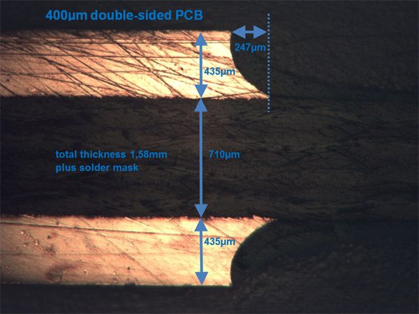
Furthermore, the distance between the traces has to be larger, so that the remaining copper can be etched down to the base material thoroughly. As you can see in the picture above the trace edges appear as rounded flanks due to multiple etch runs. This is also called "undercut". With around 250 µm per edge this is a reasonable result and will be compensated for during our CAM layout preparation. A 2 mm trace will therefore be enlarged to 2,5 mm prior to manufacturing. In order to compensate for the added width we require wider distances. For the current limits, please check the rigid PCB technologies table.
Furthermore, the distance between the traces has to be larger, so that the remaining copper can be etched down to the base material thoroughly. As you can see in the picture above the trace edges appear as rounded flanks due to multiple etch runs. This is also called "undercut". With around 250 µm per edge this is a reasonable result and will be compensated for during our CAM layout preparation. A 2 mm trace will therefore be enlarged to 2,5 mm prior to manufacturing. In order to compensate for the added width we require wider distances. For the current limits, please check the rigid PCB technologies table.
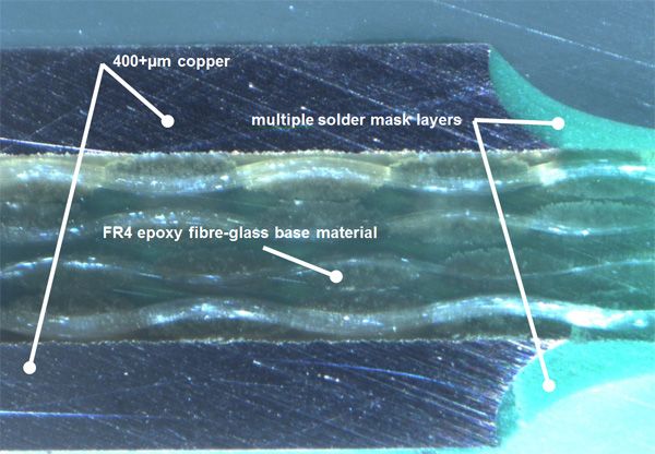
Another challenge in 400 µm PCB manufacturing is an even solder mask application that covers all edges sufficiently and appears smooth and glossy. Some other PCB producers even explicitly exclude the proper coverage of the copper edges. Thus, it is essential to apply solder mask multiple times to assure all edges are covered properly. The amount of solder mask applications and the process depend on the layout. Solder mask thicknesses on some areas can reach 250 µm per side. This explains the thickness tolerance of -10/+20% for 400 µm printed circuits.
What sounds easy is a complex task in production. Each solder mask layer has to be cured, exposed and developed separately. During these multiple solder mask applications you must make sure that the lower layers of lacquer do not emit further gasing, which would inevitably lead to bubbles. Other manufacturers commonly deliver very uneven, bubbly solder masks that is purely functional but looks rather "wild". As you can see in above picture, we perfected theses multiple solder mask layer steps for 400 µm PCBs so that it appears even and glossy as usual. If you compare our quality with other suppliers, you will see the difference.
| Material Type | FR4 Tg 150°C with thick copper cladding, thickness tolerance -10/+20% |
| Copper Thickness | 200 to 400 µm |
| Total PCB Thickness | 1,0 mm to 4,8 mm |
| Solder Mask Thickness | depends on layout, between 50 µm and 250 µm pre side |
| possible current on a 1,2mm wide 400 µm trace (example) | ca. 20 A with additional heating of ~45°C |
| Heat Conductance Copper | ca. 380 W/mk |
| Heat Conductance FR4 | ca. 0,4 W/mK |
| Maximum Layer Count | 2 layers 400 µm outer, multilayer with inner layers 35 to 105 µm |
| Flammability | UL-94 V-0 |